📚 Interacting with a Port and Pin on the STM32G0B1RE
🎯 Learning Objectives
By the end of this lesson, you will:
- Understand how to enable GPIO clocks
- Configure pins as input or output
- Write to and read from pins using registers
- Blink LEDs and respond to a button press — all in bare metal programming
1️⃣ Project Setup in Segger Embedded Studio
- Create a new project for an STM32G0B1RE target.
- Add the CMSIS device header for STM32G0 (stm32g0b1xx.h) — this gives you access to the register definitions.
2️⃣ Enable Peripheral Clocks
- Before using GPIO, you must enable its clock in the RCC (Reset and Clock Control).
//Enable power interface clock (RM 5.4.15)
RCC->APBENR1 |= RCC_APBENR1_PWREN;
//Peripherals clock enable (RM 5.4.13)
RCC->IOPENR |= RCC_IOPENR_GPIOAEN; // Port A
RCC->IOPENR |= RCC_IOPENR_GPIOBEN; // Port B
RCC->IOPENR |= RCC_IOPENR_GPIOCEN; // Port C
📌 Why? If the clock to a peripheral is not enabled, its registers won’t respond — it’s like trying to talk to a device that’s powered off
3️⃣ Configure Pin Modes
Each GPIO pin has a MODER register field:
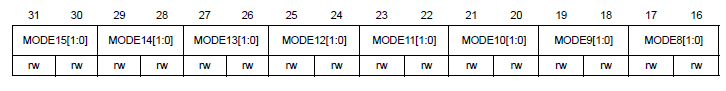
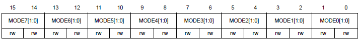
- 00 = Input
- 01 = General purpose output
- 10 = Alternate function
- 11 = Analog
Example: Set PB3 as output:
GPIOB->MODER &= ~GPIO_MODER_MODE3_Msk; // Clear mode bits
GPIOB->MODER |= GPIO_MODER_MODE3_0;    // Set to output (01)
Do the same for:
- PC6 → Output
- PB5 → Output
- PC13 → Input (just clear bits, no set)
4️⃣ Writing to Output Pins
The ODR (Output Data Register) controls pin states:
To SET
GPIOB->ODR |= GPIO_ODR_OD3; // Set PB3 high
GPIOC->ODR |= GPIO_ODR_OD6; // Set PC6 high
To TOGGLE
GPIOB->ODR ^= GPIO_ODR_OD3; // Flip PB3
To CLEAR
GPIOC->ODR &= ~GPIO_ODR_OD6; // CLear PC6
5️⃣ Reading from Input Pins
The IDR (Input Data Register) holds the current pin state:
if (GPIOB->IDR & GPIO_IDR_ID4)
{
    // PB4 is high
}
else
{
    // PB4 is low
}
✅ Key Takeaways
- Always enable the peripheral clock before using GPIO.
- Configure pin mode via MODER.
- Use ODR to write, IDR to read.
- Bare-metal programming means direct register acces.