📚 Microcontroller Core: Arm Cortex-M0+
The STM32G0B1RE is built around the Arm Cortex-M0+ processor core.
- Arm designs the core architecture.
- It’s optimized for low-power, cost-sensitive embedded applications.
- The Cortex-M0+ is widely used across many vendors.
1️⃣ MCU Vendor: STMicroelectronics
While Arm provides the core design, STMicroelectronics integrates it into a complete microcontroller:
- Adds peripherals (GPIO, ADC, timers, etc.)
- Configures memory (Flash, RAM)
- Provides development tools and documentation Other vendors also use Arm cores:
- NXP (e.g., LPC series)
- Texas Instruments (e.g., MSP432)
- Raspberry Pi Pico (RP2040)
- Nordic, Silicon Labs, and more
🎮 Analogy: GPU Chipsets and Graphics Cards
Think of it like this:
- Nvidia designs the GeForce GPU chipset.
- Companies like Asus, Gigabyte, and MSI build graphics cards around it.
- Same core, different implementations.
👉 Similarly:
- Arm designs the Cortex-M0+ core.
- STMicroelectronics builds the STM32 MCU around it.
2️⃣ Standardization: CMSIS
To make development easier across different vendors, Arm introduced CMSIS:
- CMSIS = Cortex Microcontroller Software Interface Standard
- Provides a consistent API for:
- Core functions
- Peripheral access
- Startup code and system configuration
- Supported by most Arm-based MCU vendors 📘 This means:
- Code written for one Cortex-M MCU can often be ported to another with minimal changes.
- You can focus on your application logic, not vendor-specific quirks
🧰 Why This Matters
Understanding these layers helps you:
- Recognize the modular nature of embedded systems.
- Appreciate vendor diversity while relying on core standardization.
- Leverage CMSIS for portable, scalable code.
3️⃣ Cortex-M0 Processor Architecture
- Cortex-M0 is a 32-bit processor designed for low-power, cost-sensitive embedded systems.
- It uses the ARMv6-M architecture, which is a simplified version of ARM’s instruction set.
4️⃣ Key Features
- Registers:
- 16 general-purpose registers (R0–R15)
- Special registers like Program Counter (PC), Link Register (LR), and Stack Pointer (SP)
- Thumb Instruction Set:
- Uses a compact 16-bit instruction format for efficiency.
- Supports basic arithmetic, logic, control flow, and memory access.
5️⃣ Pipeline
- 3-stage pipeline: Fetch → Decode → Execute
- Improves performance while keeping power consumption low.
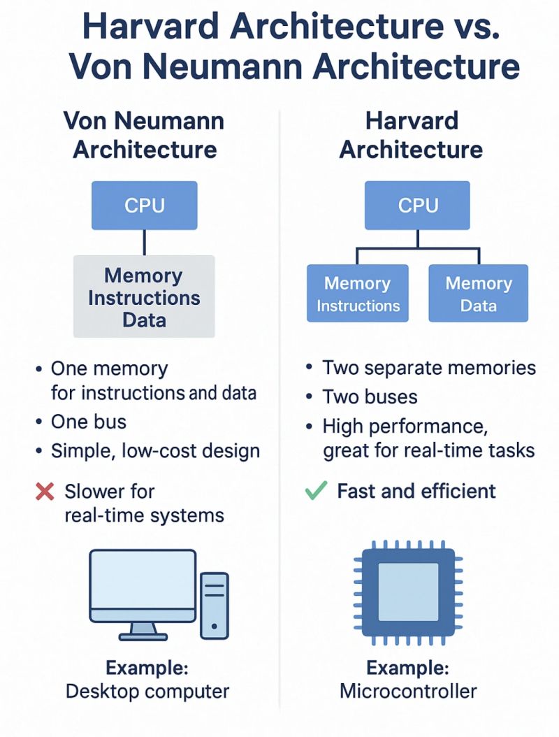
6️⃣ Memory System
- Harvard architecture: separate instruction and data buses.
- Supports bit-band operations for atomic bit-level access.
- Includes SysTick timer for simple timekeeping.
7️⃣ Exception Handling
- Supports interrupts and exceptions with automatic context saving.
- Uses a vector table to manage interrupt service routines (ISRs).
8️⃣ Debug Support
- Includes basic debug features like breakpoints and single-step execution.
- Compatible with Serial Wire Debug (SWD) interface.