📚 CMPE1250: Reset and Clock Control (RCC)
🎯 Learning Objectives
By the end of this lesson, students will be able to:
- Explain the role of the RCC in the STM32 microcontroller.
- Identify the different reset sources and their effects.
- Describe the available clock sources (HSI, HSE, LSI, LSE, PLL).
- Configure the system clock (SYSCLK) and peripheral clocks using registers.
- Write simple C code to switch between clock sources and verify operation.
1️⃣ Why Do We Need a Clock System?
- To power the MCU and different peripherals such as timers, USART, ADC, etc.
- Some peripherals will require more precise clock, such as USB or RTC.
- Some other will require an acceptable clock
2️⃣ Reset Sources
| Reset Type | Trigger | Effect |
|---|---|---|
| Power Reset | Power-on, brown-out, exit Standby/Shutdown | All registers reset except RTC domain |
| System Reset | NRST pin, watchdogs, software reset | Most registers reset, RTC domain preserved |
| RTC Reset | Software (BDRST) or VBAT/VDD loss | Only RTC, backup registers, LSE affected |
👉 Key Register: RCC_CSR holds reset flags so you can check why the MCU restarted.
3️⃣ Clock Sources
The STM32G0 provides several oscillators and clock sources:
| Clock Source | Type | Frequency Range | Availability | Typical Use |
|---|---|---|---|---|
| HSI16 | Internal RC oscillator | 16 MHz (±1% factory calibrated) | All STM32G0 devices | Default SYSCLK, backup clock, USART/I²C/SPI |
| HSE | External crystal/clock | 4–48 MHz | Not available on STM32G031/G030 (only on larger G0x1, G0B1, G0C1) | Precise SYSCLK, USB, CAN, accurate baud rates |
| HSI48 | Internal RC oscillator | 48 MHz | Only STM32G0B1/G0C1 | USB, RNG (with CRS for precision) |
| LSE | External crystal/clock | 32.768 kHz (up to 1 MHz in bypass) | All STM32G0 devices (OSC32_IN/OSC32_OUT pins) | RTC, low-power timing |
| LSI | Internal RC oscillator | ~32 kHz | All STM32G0 devices | Watchdog (IWDG), backup RTC clock |
| PLL | Internal frequency multiplier/divider | Input: 2.66–16 MHz → up to 64 MHz SYSCLK | All STM32G0 devices | Flexible SYSCLK and peripheral clocks |
-
HSI: High Speed Internal -
HSE: High Speed External (Oscilator or Crystal: 4[MHz] - 48[MHz]) -
LSI: Low Speed Internal -
LSE: Low Speed External (32[KHz] Crystal) -
PLL: Phase-Locked Loop
Notes
- On STM32G031/G030, there are no HSE pins (OSC_IN/OSC_OUT). Only HSI16, LSI, and LSE are available.
- On STM32G0B1/G0C1, you also get HSI48 for USB and RNG.
- The PLL can take HSI16 or HSE as input (when available) and generate multiple outputs (PLLPCLK, PLLQCLK, PLLRCLK).
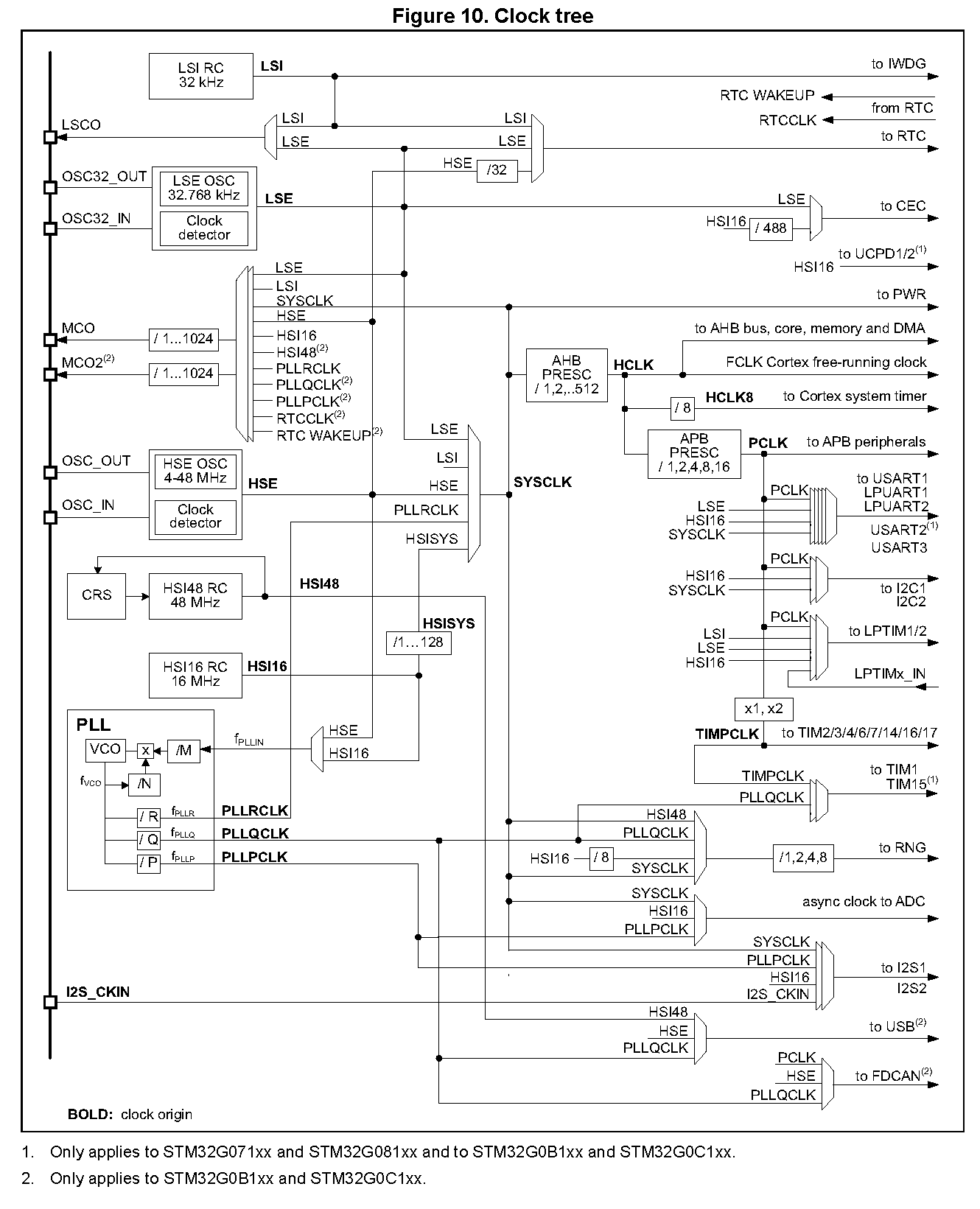
4️⃣ Clock Tree Overview
5️⃣ Hands-On: Switching the System Clock
- The main clock is SYSCLK.
- After reset, the defaults to use HSI16 (16MHz) as the clock source for SYSCLK.
- To enable any other clock source, that has to be done in the CR register of the RCC. For instance, to enable HSE as the clock source, if there was one populated:
Step 1: Enable HSE
RCC->CR |= RCC_CR_HSEON;              // Turn on HSE
while (!(RCC->CR & RCC_CR_HSERDY));   // Wait until stable
Step 2: Switch SYSCLK to HSE
RCC->CFGR &= ~RCC_CFGR_SW;            // Clear clock switch bits
RCC->CFGR |= RCC_CFGR_SW_HSE;         // Select HSE as SYSCLK
while ((RCC->CFGR & RCC_CFGR_SWS) != RCC_CFGR_SWS_HSE); // Wait for switch
6️⃣ Verifying the clock speed
✅ Method 1: CMSIS Function (SystemCoreClock)
Steps:
- Call the CMSIS function:
SystemCoreClockUpdate();           // Updates the SystemCoreClock variable
uint32_t sysclk = SystemCoreClock; // Holds the current SYSCLK in Hz
- Print or log the value:
printf("SYSCLK = %lu Hz\n", sysclk);
Notes:
- SystemCoreClock is updated based on register values (RCC_CFGR, RCC_PLLCFGR, etc.).
- Always call SystemCoreClockUpdate() after changing clock configuration.
✅ Method 2: MCO Pin Output
This is the hardware-based way to verify SYSCLK using an oscilloscope or frequency counter.
Steps:
- Configure MCO pin (e.g., PA8 on STM32G031)
RCC->CFGR &= ~RCC_CFGR_MCOSEL;        // Clear MCO source
RCC->CFGR |= RCC_CFGR_MCOSEL_SYSCLK;  // Select SYSCLK as MCO source

RCC->CFGR &= ~RCC_CFGR_MCOPRE;        // Clear prescaler
RCC->CFGR |= RCC_CFGR_MCOPRE_DIV1;    // No division

// Enable GPIOA and configure PA8 as alternate function
RCC->IOPENR |= RCC_IOPENR_GPIOAEN;

GPIO_InitAlternateF(GPIOA, 8, 0);

/*Manual implementation of the line above*/
GPIOA->MODER &= ~(3 << (8 * 2));
GPIOA->MODER |=  (2 << (8 * 2));       // AF mode
GPIOA->AFR[1] &= ~(0xF << ((8 - 8) * 4));
GPIOA->AFR[1] |=  (0x0 << ((8 - 8) * 4)); // AF0 = MCO
- Measure the frequency at the PIN (such as PA8) using an oscilloscope.
Notes:
-
You can also output other clocks (HSI16, HSE, PLLRCLK) by changing
MCOSEL. -
Use
MCOPREto divide the output if your scope has bandwidth limits.
7️⃣ Using the PLL as the System Clock
- General formula:
$f_{\text{PLL}} = \frac{f_{\text{input}}}{M} \cdot \frac{N}{X}$
- X is R, Q or P
Where:
- $f_{\text{input}}$ = input clock frequency (HSI16 = 16 MHz or HSE = 4–48 MHz)
- M = input divider (1 to 8)
- N = multiplier (integer, chosen to reach VCO frequency)
- R = output divider:
- R for PLLRCLK (used for SYSCLK)
- Q for PLLQCLK (used for USB, RNG, timers)
- P for PLLPCLK (used for ADC, I²S)
Formula for system clock using the PLL:
$f_{\text{PLL}} = \frac{f_{\text{input}}}{M} \cdot \frac{N}{R}$
VCO Frequency Constraint
The intermediate VCO frequency must satisfy:
$f_{\text{VCO}} = \frac{f_{\text{input}}}{M} \cdot N$
- Must be within:
- 128–344 MHz for Range 1
- 128 MHz max for Range 2
✅ SYSCLK via PLLRCLK summary
For Pll Configuration check (5.2.4) in the Reference Manual Also, the Clock Configuration tab in STMCubeMx.
PLL_CLK = PLL_IN x (N / M) / R
The PLL PLL_CLK frequency must not exceed 64 MHz
The following configurations get done in the RCC_PLLCFGR register:
(1) PLL_IN, depends on PLLSRC BITS[1:0] - PLLSRC = 0 (HSI16 Clock) //16MHZ - PLLSRC = 1 (HSE Clock) //Given by external crystal
(2) N depends on PLLN BITS[14:8]
(3) M depends on PLLM BITS[6:4]
(4) R depends on PLLR BITS[31:29]
✅ Example: SYSCLK via PLLRCLK
Let’s say:
- Input = HSI16 = 16 MHz
- M = 2, N = 20, R = 5
Then:
- $f_{\text{VCO}} = \frac{16}{2} \cdot 20 = 160\,\text{MHz}$
- $f_{\text{PLLRCLK}} = \frac{160}{5} = 32\,\text{MHz}$
So your SYSCLK would be 32 MHz.
✅ Detailed steps to configure PLL
-
Disable PLL (
PLLONinRCC->CR) -
Wait until Pll is fully stopped (
PLLRDYinRCC->CR) -
Write pllRange (
N, M, R) and selectHSIinRCC->PLLCFGR -
Enable PLL again (
PLLONinRCC->CR) -
Wait until PLL is locked (
PLLRDYinRCC->CR) -
Enable PLL peripheral and PLLR outputs (
PLLPENandPLLRENinRCC->PLLCFGR) -
Set Pll as System Clock (
SW_PLLinRCC->CFGR) -
Enable MCO line as discussed in class to verify clock speed
- Remember to add these to lines to slow down the flash access and enable intruction prefetch:
  /*Define HCLK clock ratio to the FLASH,
    slow down system to access flash (RM 3.7.1)*/
  FLASH->ACR |= FLASH_ACR_PRFTEN_Msk;     //Enable instruction prefetch
  FLASH->ACR |= FLASH_ACR_LATENCY_Msk;    //One wait state is used to read a word in the NVM.
✅ Practical activity
- Set the PLL to 40MHz
- Follow the preious steps and the following
RCC->PLLCFGR = (RCC_PLLCFGR_PLLSRC_HSI | (M-1)<<4 | N<<8 | (R-1)<<29);
RCC->CR |= RCC_CR_PLLON;
while (!(RCC->CR & RCC_CR_PLLRDY));
Then switch SYSCLK to PLLRCLK via RCC_CFGR.