📚 CMPE2250: Lesson — Serial Peripheral Interface (SPI) on STM32G0
🎯 Overview
-
The Serial Peripheral Interface (SPI) is a simple, highly configurable serial communication interface that supports standard synchronous protocols.
-
Applications benefit from its direct connection to external components, requiring only a few pins.
-
In our embedded systems projects, SPI provides a robust way to interface with displays, smart sensors, memories, and SD cards.
Key Features
- Operating Modes: Nodes can be configured as a Master or a Slave.
- Directionality: The bus supports full-duplex, simplex, or half-duplex communication.
- Speed: Communication operations can run up to half of the internal bus frequency ($f_{PCLK}/2$).
- Data Frame: The data frame size is fully programmable and flexible, ranging from 4 up to 16 bits.
1️⃣ Hardware Interconnections
In a standard SPI bus, the Master controls the traffic and provides the clock signal to the dedicated slave through the SCK line.
A typical full-duplex setup uses four distinct lines:
-
SCK (Serial Clock): Generated by the Master to synchronize data. -
MOSI (Master Output, Slave Input): Transmits data from the Master to the Slave. -
MISO (Master Input, Slave Output): Transmits data from the Slave to the Master. -
SS / NSS (Slave Select): Used by the Master to select the specific slave it wants to communicate with.
When connecting multiple slaves, a Star Topology is commonly used. In this topology, a separate Slave Select signal from the master has to be provided to each slave node via a dedicated GPIO pin.
2️⃣ Clock Polarity and Phase (CPOL & CPHA)
To ensure reliable synchronous data transfer, the master and slave must agree on the clock format. There are four basic configurations defined in the Motorola SPI specifications. These configurations are controlled by two parameters:
-
CPOL (Clock Polarity): Defines the idle state of the clock signal and which clock edge is used for data sampling.-
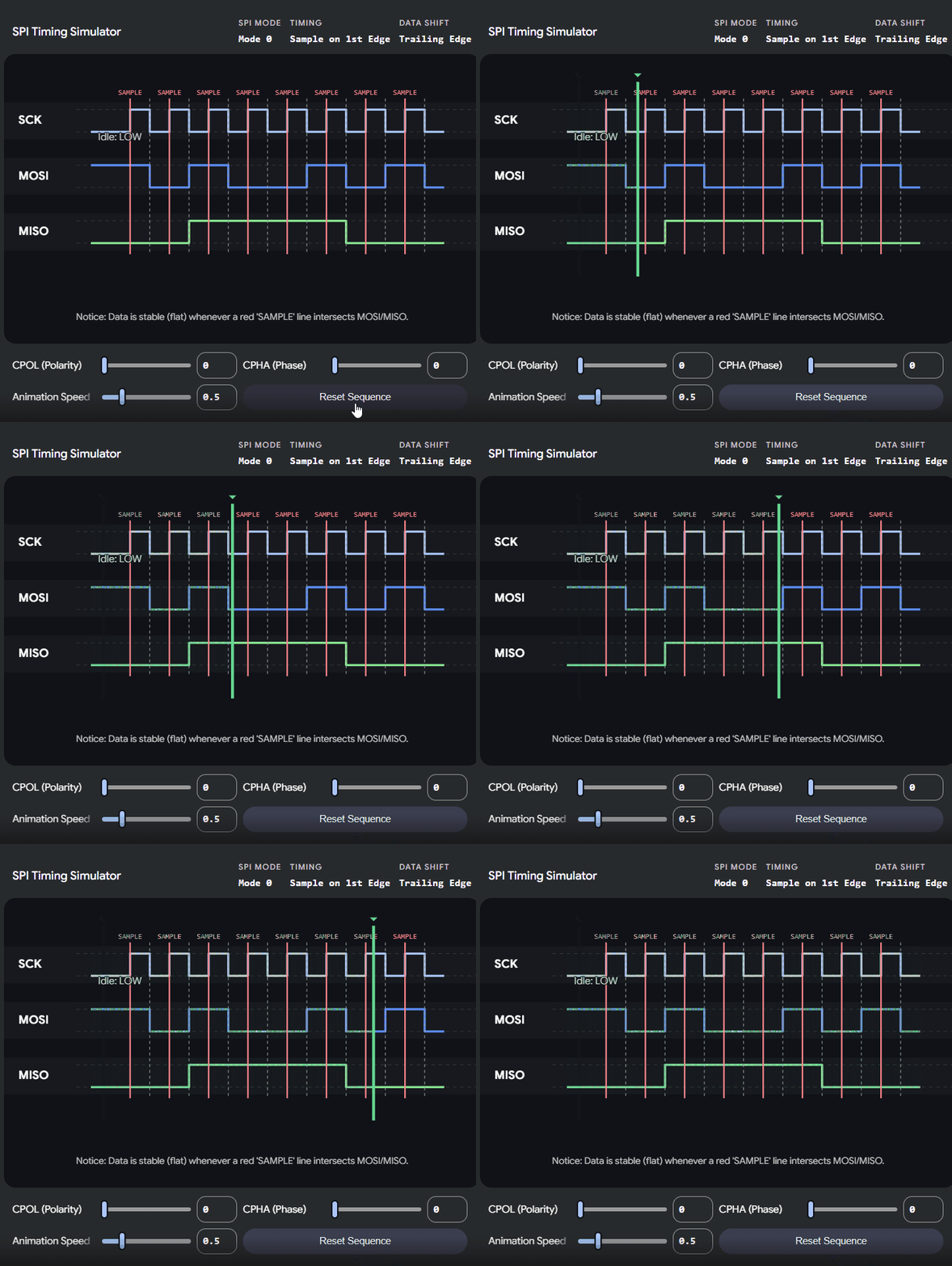
CPOL = 0: Clock idles low. -
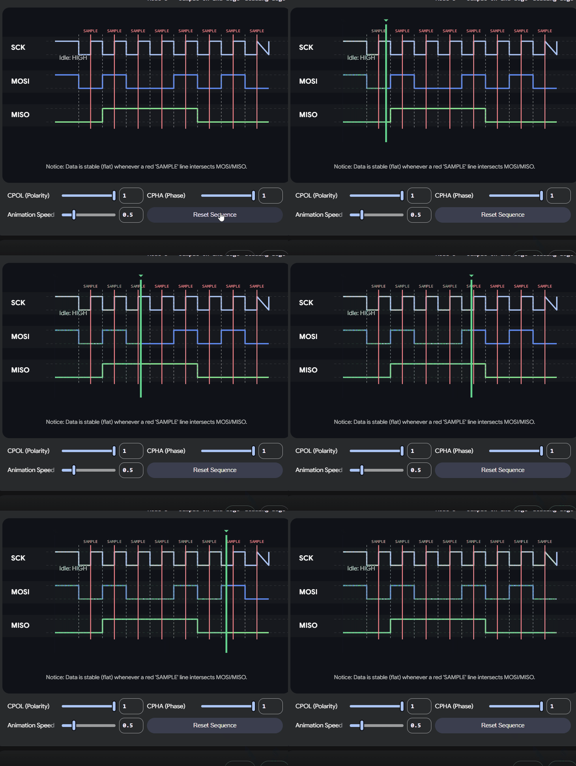
CPOL = 1: Clock idles high.
-
-
CPHA (Clock Phase):-
CPHA = 0: Data bits are sampled on the odd clock edges. The even clock edges synchronize the shifting of the next bit onto the data line. -
CPHA = 1: Data bits are sampled on the even clock edges, which is the opposite behavior.
-
Understanding the relationship between CPOL and CPHA is critical when writing drivers for external peripherals. The interactive diagram below allows you to explore how changing the polarity and phase shifts the sampling edges during an SPI transaction.
Clock Polarity and Phase (CPOL = 0 CPHA = 0)
 .
.
Clock Polarity and Phase (CPOL = 1 CPHA = 1)
 .
.
3️⃣ STM32G0 SPI Implementation (Blocking Mode)
- Below is a practical example of configuring SPI2 as a master in blocking mode on the STM32G0. In this configuration, we transmit a byte (0x82) periodically using the SysTick_Handler.
int main(void)
{
  // Initialization & Clock Enable
  RCC->APBENR1 |= RCC_APBENR1_PWREN;
  RCC->IOPENR  |= RCC_IOPENR_GPIOAEN | RCC_IOPENR_GPIOBEN | RCC_IOPENR_GPIOCEN;
  RCC->APBENR1 |= RCC_APBENR1_SPI2EN; // Enable SPI2 clock

  Clock_InitPll(PLL_40MHZ);
  SysTick_Config(SystemCoreClock / 1000);  // 1[ms] ticks

  // SPI GPIO Configuration
  GPIO_InitOutput(GPIOB, 10);           // CS (Chip Select)
  GPIO_Set(GPIOB, 10);                  // Start with CS high (deselected)
  GPIO_InitAlternateF(GPIOB, 13, 0);    // SPI2_CK
  GPIO_InitAlternateF(GPIOC, 2, 1);     // SPI2_MISO
  GPIO_InitAlternateF(GPIOC, 3, 1);     // SPI2_MOSI

  // SPI Peripheral Configuration
  SPI2->CR1 &= ~SPI_CR1_BR;             // Clear BR settings
  SPI2->CR1 |= SPI_CR1_BR_1;            // Divide PCLK by 8 -> 5[MHz]
  SPI2->CR1 |= SPI_CR1_CPOL | SPI_CR1_CPHA;  // Set mode to (1,1)
  SPI2->CR1 |= SPI_CR1_MSTR;            // Master Configuration
  SPI2->CR1 |= SPI_CR1_SSM | SPI_CR1_SSI;    // Software Slave Management enabled

  // 8-bit data size configuration
  SPI2->CR2 |= SPI_CR2_DS_2 | SPI_CR2_DS_1 | SPI_CR2_DS_0;
  SPI2->CR2 |= SPI_CR2_FRXTH;           // RXNE generated on 8-bit data event
  SPI2->CR1 |= SPI_CR1_SPE;             // Enable SPI

  while(1) {
    // Infinite loop. Handled in SysTick
  }
}

void SysTick_Handler(void)
{
  uint8_t rxData;

  GPIO_Clear(GPIOB, 10); // 1. Pull CS Low to initiate communication

  while(!(SPI2->SR & SPI_SR_TXE)); // 2. Wait until TX register is empty

  // 3. Force 8-bit write access to the Data Register
  *((__IO uint8_t*)(&SPI2->DR)) = 0x82;

  while(!(SPI2->SR & SPI_SR_RXNE)); // 4. Wait until RX register has data

  // 5. Read the incoming byte
  rxData = SPI2->DR;

  GPIO_Set(GPIOB, 10); // 6. Pull CS High to terminate communication
}
Code Walkthrough
-
Hardware Initialization: The system clock is brought up to 40 MHz, and the peripheral clocks for the required GPIO ports and SPI2 are enabled via the RCC registers.
-
Pin Multiplexing:
-
PB10 is set as a standard output to manually drive the Chip Select line (CS). It’s initialized high (idle).
-
PB13, PC2, and PC3 are set to their Alternate Function modes so the internal SPI2 hardware can take control of them.
-
-
SPI Control Register 1 (CR1):
-
Baud Rate: Dividing the 40 MHz clock by 8 yields a 5 MHz SPI clock.
-
Clock Mode: Setting both CPOL and CPHA configures the bus for SPI Mode 3.
-
Slave Management: SSM and SSI bits are set to handle the CS pin manually via software, rather than relying on the hardware’s automatic NSS management.
-
-
SPI Control Register 2 (CR2):
-
We set the Data Size (DS) to 8 bits.
-
Setting FRXTH ensures that the RXNE (Receive Buffer Not Empty) flag triggers appropriately when a single 8-bit byte is received.
-
-
The Transaction (SysTick): Every millisecond, the interrupt fires. We pull CS low, wait for the transmit buffer to clear (TXE), and write 0x82 to the Data Register. Notice the explicit (__IO uint8_t*) pointer cast—this is a best practice to force the compiler into an 8-bit memory access, keeping the data frames properly packed. We then wait for the RXNE flag before reading the incoming byte and pulling CS back high.