📚 Chapter 2: Introduction to RS232 Serial Communication
🎯 Learning Objectives
By the end of this lesson, students will be able to:
- Explain the purpose and characteristics of RS‑232 signaling
- Interpret RS‑232 voltage levels, logic inversion, and idle states
- Describe asynchronous framing (start, data, parity, stop)
- Configure a serial port correctly (baud, data bits, parity, stop bits, flow control)
- Perform a loopback test using HyperTerminal
- Build and use a simple breakout box (BOB)
- Observe RS‑232 signals using an oscilloscope and/or protocol analyzer
- Decode RS‑232 waveforms to identify transmitted ASCII characters (Assignment 2)
1️⃣ What is RS232 Serial Communication
RS‑232 is an asynchronous serial communication standard originally designed for connecting computers and modems. Despite its age, it remains widely used in:
- industrial automation
- PLCs
- embedded systems
- instrumentation
- legacy equipment
It defines:
- Voltage levels
- Logic polarity
- Signal names and pinouts
- Framing rules
- Handshaking lines
It does not define:
- Connectors
- Baud rates
- ASCII vs binary
- Cable length
- Protocols above the physical layer
2️⃣ RS‑232 Voltage Levels and Logic
RS‑232 uses bipolar, inverted logic:
| Logical Meaning | RS‑232 Voltage | Name |
|---|---|---|
| 1 (MARK) | −3 V to −15 V | Idle, Stop |
| 0 (SPACE) | +3 V to +15 V | Start, Data “0” |
Key points:
- Idle line = MARK = logic 1 = negative voltage
- Start bit = SPACE = logic 0 = positive voltage
- Data bits follow LSB first
- Stop bit(s) return to MARK (negative)
This inversion is why the Analog Discovery 2 Protocol Analyzer must be set to Inverted Polarity.
3️⃣ DTE vs DCE
RS‑232 defines two device types:
| Device Type | Description | Examples |
|---|---|---|
| DTE (Data Terminal Equipment) | A device that generates and receives data, such as a computer or terminal | Computer, Terminal |
| DCE (Data Circuit-terminating Equipment) | A device that provides the interface to the communication medium, such as a modem | Modem, Interface Card |
Signal directions are defined relative to the DTE.
This is why:
- PC TXD → DCE RXD
- PC RXD ← DCE TXD
When connecting two DTEs, you need a null modem (crossed TX/RX).
flowchart LR
    subgraph DTE["DTE (PC or MCU)"]
        TXD_DTE[TXD - Transmit Data]
        RXD_DTE[RXD - Receive Data]
    end

    subgraph DCE["DCE (Modem or USB-Serial)"]
        RXD_DCE[RXD - Receive Data]
        TXD_DCE[TXD - Transmit Data]
    end

    TXD_DTE --> RXD_DCE
    TXD_DCE --> RXD_DTE
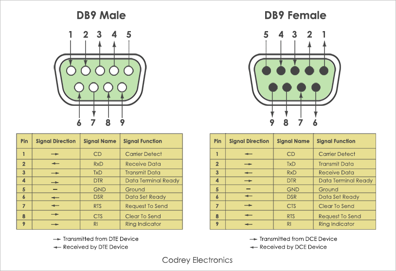
4️⃣ DB‑9 Pinout (as used in Lab01)
| Pin | Name | Direction | |
|---|---|---|---|
| 1 | DCD (Data Carrier Detect) | IN Modem | |
| 2 | RXD (Receive Data) | IN PC, OUT Modem | |
| 3 | TXD (Transmit Data) | OUT PC, IN Modem | |
| 4 | DTR (Data Terminal Ready) | OUT PC | |
| 5 | GND (Ground) | N/A | GND |
| 6 | DSR (Data Set Ready) | IN Modem | |
| 7 | RTS (Request To Send) | OUT PC | |
| 8 | CTS (Clear To Send) | IN PC | |
| 9 | RI (Ring Indicator) | IN Modem |
For Lab01, only pins 2, 3, and 5 are used.
5️⃣ Asynchronous Framing (Needed for Assignment 2)
Every character is wrapped in a frame:
Start | Data bits (LSB→MSB) | Parity (optional) | Stop bit(s)
flowchart LR
    Idle[Idle - MARK = 1]
    Start[Start bit - 0]
    B0[Bit 0 - LSB]
    B1[Bit 1]
    B2[Bit 2]
    B3[Bit 3]
    B4[Bit 4]
    B5[Bit 5]
    B6[Bit 6 - MSB]
    Parity[Parity bit]
    Stop[Stop bit - 1]

    Idle --> Start
    Start --> B0
    B0 --> B1
    B1 --> B2
    B2 --> B3
    B3 --> B4
    B4 --> B5
    B5 --> B6
    B6 --> Parity
    Parity --> Stop
Example: 7‑bit ASCII, Even parity, 1 stop bit
0 d0 d1 d2 d3 d4 d5 d6 P 1
Where:
- Start bit = 0 (SPACE, + voltage)
- Stop bit = 1 (MARK, − voltage) Students must decode waveforms by:
- Identifying the start bit (first positive transition)
- Sampling LSB first
- Counting 1s to determine parity correctness
- Reversing bit order to get the ASCII code This is exactly what Assignment 2 asks.
6️⃣ Configuring a Serial Port
For Lab01:
- 9600 baud
- 8 data bits
- No parity
- 1 stop bit
- No flow control These settings must match the microcontroller or loopback test.
7️⃣ Loopback Testing (Lab01)
A loopback test verifies:
- Serial adapter/cable works
- Terminal is configured correctly
- TXD and RXD are functional
Procedure:
- Connect TXD → RXD on the breakout box
- Enable local echo in Terminal
- Type your name
- You should see two copies of each character
- one local
- one looped back
This is required for Lab01 Question 3.
8️⃣ Building the Simple Breakout Box (BOB)
Students wire:
- LEDs + resistors on TXD and RXD
- Ground reference
- Optional: handshaking lines
Purpose:
- Visualize MARK (idle) and SPACE (activity)
- Observe direction of data flow
- Debug wiring errors When both directions are active (full‑duplex), all LEDs flicker
flowchart LR
    subgraph BOB ["Simple Breakout Box"]
        RXD["RXD (Pin 2)"]
        TXD["TXD (Pin 3)"]
        GND["GND (Pin 5)"]

        LED1["LED1 on RXD"]
        LED2["LED2 on RXD"]
        LED3["LED3 on TXD"]
        LED4["LED4 on TXD"]

        RXD --> LED1
        RXD --> LED2
        TXD --> LED3
        TXD --> LED4
    end
9️⃣ Observing RS‑232 Signals (Oscilloscope / AD2)
Students must:
- Connect CH1 → TXD
- Connect CH2 → RXD
- Trigger on falling edge (start bit)
- Hold down a key (e.g., “u”)
- Capture waveform
They should see:
- Idle negative voltage
- Start bit positive
- LSB first
- Stop bit negative
This prepares them for Assignment 2 waveform decoding.
🔟 Using the Protocol Analyzer (AD2)
Settings: • UART mode • Inverted polarity • 9600 baud • 8‑N‑1 • Text mode • Vertical view (TX/RX separated)
You will see: • Lowercase “u” from HyperTerminal • Uppercase “U” echoed back by the microcontroller (case‑flip program)
This reinforces: • Full‑duplex • Framing • ASCII codes • Logic inversion